Tahiti!.. Tahiti!..
We have not been to any Tahiti!
They feed us well here too!
© Cartoon cat
Introduction with digression
How were boards made in the past in domestic and laboratory conditions? There were several ways, for example:
- future conductors drew drawings;
- engraved and cut with cutters;
- they glued it with adhesive tape or tape, then cut out the design with a scalpel;
- They made simple stencils and then applied the design using an airbrush.
The missing elements were completed with drawing pens and retouched with a scalpel.
It was a long and laborious process, requiring the “drawer” to have remarkable artistic abilities and accuracy. The thickness of the lines hardly fit into 0.8 mm, there was no repetition accuracy, each board had to be drawn separately, which greatly limited the production of even a very small batch printed circuit boards(further PP).
What do we have today?
Progress does not stand still. The times when radio amateurs painted PP with stone axes on mammoth skins have sunk into oblivion. The appearance on the market of publicly available chemistry for photolithography opens up completely different prospects for the production of PCB without metallization of holes at home.
Let's take a quick look at the chemistry used today to produce PP.
Photoresist
You can use liquid or film. We will not consider film in this article due to its scarcity, difficulties in rolling onto PCBs and the lower quality of the resulting printed circuit boards.
After analyzing market offers, I settled on POSITIV 20 as the optimal photoresist for home PCB production.
Purpose:
POSITIV 20 photosensitive varnish. Used in small-scale production of printed circuit boards, copper engravings, and when carrying out work related to transferring images to various materials.
Properties:
High exposure characteristics provide good contrast of transferred images.
Application:
It is used in areas related to the transfer of images onto glass, plastics, metals, etc. in small-scale production. Directions for use are indicated on the bottle.
Characteristics:
Color: blue
Density: at 20°C 0.87 g/cm 3
Drying time: at 70°C 15 min.
Consumption: 15 l/m2
Maximum photosensitivity: 310-440 nm
The instructions for the photoresist say that it can be stored at room temperature and is not subject to aging. I strongly disagree! It should be stored in a cool place, for example, on the bottom shelf of the refrigerator, where the temperature is usually maintained at +2+6°C. But under no circumstances allow negative temperatures!
If you use photoresists that are sold by the glass and do not have lightproof packaging, you need to take care of protection from light. It should be stored in complete darkness and at a temperature of +2+6°C.
Enlightener
Likewise, I consider TRANSPARENT 21, which I constantly use, to be the most suitable educational tool.
Purpose:
Allows direct transfer of images onto surfaces coated with photosensitive emulsion POSITIV 20 or other photoresist.
Properties:
Gives transparency to paper. Provides transmission of ultraviolet rays.
Application:
For quickly transferring the outlines of drawings and diagrams onto a substrate. Allows you to significantly simplify the reproduction process and reduce time s e costs.
Characteristics:
Color: transparent
Density: at 20°C 0.79 g/cm 3
Drying time: at 20°C 30 min.
Note:
Instead of regular paper with transparency, you can use transparent film for inkjet or laser printers, depending on what we will print the photomask on.
Photoresist developer
There are many different solutions for developing photoresist.
It is recommended to develop using a “liquid glass” solution. Its chemical composition: Na 2 SiO 3 * 5H 2 O. This substance has a huge number of advantages. The most important thing is that it is very difficult to overexpose the PP in it; you can leave the PP for a non-fixed exact time. The solution almost does not change its properties with temperature changes (there is no risk of decay when the temperature increases), and also has a very long shelf life - its concentration remains constant for at least a couple of years. The absence of the problem of overexposure in the solution will allow increasing its concentration to reduce the time of development of PP. It is recommended to mix 1 part concentrate with 180 parts water (just over 1.7 g of silicate in 200 ml of water), but it is possible to make a more concentrated mixture so that the image develops in about 5 seconds without the risk of surface damage due to overexposure. If it is impossible to purchase sodium silicate, use sodium carbonate (Na 2 CO 3) or potassium carbonate (K 2 CO 3).
I haven’t tried either the first or the second, so I’ll tell you what I’ve been using without any problems for several years now. I use a water solution of caustic soda. For 1 liter of cold water 7 grams of caustic soda. If there is no NaOH, I use a KOH solution, doubling the concentration of alkali in the solution. Development time 30-60 seconds with correct exposure. If after 2 minutes the pattern does not appear (or appears weakly), and the photoresist begins to wash off from the workpiece, this means that the exposure time was chosen incorrectly: you need to increase it. If, on the contrary, it quickly appears, but both exposed and unexposed areas are washed away; either the concentration of the solution is too high, or the quality of the photomask is low (ultraviolet light passes freely through the “black”): you need to increase the print density of the template.
Copper etching solutions
Excess copper is removed from printed circuit boards using various etchants. Among people doing this at home, ammonium persulfate, hydrogen peroxide + hydrochloric acid, copper sulfate solution + table salt are often common.
I always poison with ferric chloride in a glass container. When working with the solution, you need to be careful and attentive: if it gets on clothes and objects, it leaves rusty stains that are difficult to remove with a weak solution of citric (lemon juice) or oxalic acid.
We heat a concentrated solution of ferric chloride to 50-60°C, immerse the workpiece in it, and carefully and effortlessly move a glass rod with a cotton swab at the end over areas where copper is etched less easily, this achieves a more even etching over the entire area of the PP. If you do not force the speed to equalize, the required etching duration increases, and this eventually leads to the fact that in areas where copper has already been etched, etching of the tracks begins. As a result, we don’t get what we wanted at all. It is highly desirable to ensure continuous stirring of the etching solution.
Chemicals for removing photoresist
What is the easiest way to wash off unnecessary photoresist after etching? After repeated trial and error, I settled on ordinary acetone. When it’s not there, I wash it off with any solvent for nitro paints.
So, let's make a printed circuit board
Where does a high quality PCB start? Right:
Create a high-quality photo template
To make it, you can use almost any modern laser or inkjet printer. Considering that we are using positive photoresist in this article, the printer should draw black where copper should remain on the PCB. Where there should be no copper the printer should not draw anything. A very important point when printing a photomask: you need to set the maximum dye flow (in the printer driver settings). The blacker the painted areas, the greater the chances of getting a great result. No color is needed, a black cartridge is enough. From the program (we will not consider programs: everyone is free to choose for themselves - from PCAD to Paintbrush) in which the photo template was drawn, we print it on a regular sheet of paper. The higher the printing resolution and the higher quality the paper, the higher the quality of the photomask. I recommend no lower than 600 dpi; the paper should not be very thick. When printing, we take into account that with the side of the sheet on which the paint is applied, the template will be placed on the PP blank. If done differently, the edges of the PP conductors will be blurred and indistinct. Let the paint dry if it was an inkjet printer. Next, we impregnate the paper with TRANSPARENT 21, let it dry and the photo template is ready.
Instead of paper and enlightenment, it is possible and even very desirable to use transparent film for laser (when printing on a laser printer) or inkjet (for inkjet printing) printers. Please note that these films have unequal sides: only one working side. If you use laser printing, I highly recommend dry running a sheet of film before printing - simply run the sheet through the printer, simulating printing, but not printing anything. Why is this necessary? When printing, the fuser (oven) will heat the sheet, which will inevitably lead to its deformation. As a consequence, there is an error in the geometry of the output PCB. When producing double-sided PCBs, this is fraught with a mismatch of layers with all the consequences And with the help of a “dry” run, we will warm up the sheet, it will be deformed and will be ready for printing the template. When printing, the sheet will pass through the oven a second time, but the deformation will be much less significant checked several times.
If the PP is simple, you can draw it manually in a very convenient program with a Russified interface Sprint Layout 3.0R (~650 KB).

At the preparatory stage, it is very convenient to draw not too cumbersome electrical circuits in the also Russified sPlan 4.0 program (~450 KB).

This is what the finished photo templates look like, printed on an Epson Stylus Color 740 printer:


We print only in black, with maximum dye addition. Material transparent film for inkjet printers.
Preparing the PP surface for applying photoresist
For the production of PP, sheet materials coated with copper foil are used. The most common options are with copper thickness of 18 and 35 microns. Most often, for the production of PP at home, sheet textolite (fabric pressed with glue in several layers), fiberglass (the same, but epoxy compounds are used as glue) and getinax (pressed paper with glue) are used. Less commonly, sittal and polycor (high-frequency ceramics are used extremely rarely at home), fluoroplastic (organic plastic). The latter is also used for the manufacture of high-frequency devices and, having very good electrical characteristics, can be used anywhere and everywhere, but its use is limited by its high price.
First of all, you need to make sure that the workpiece does not have deep scratches, burrs or corroded areas. Next, it is advisable to polish the copper to a mirror. We polish without being particularly zealous, otherwise we will erase the already thin layer of copper (35 microns) or, in any case, we will achieve different thicknesses of copper on the surface of the workpiece. And this, in turn, will lead to different etching rates: it will be etched faster where it is thinner. And a thinner conductor on the board is not always good. Especially if it is long and a decent current will flow through it. If the copper on the workpiece is of high quality, without sins, then it is enough to degrease the surface.
Applying photoresist to the surface of the workpiece
We place the board on a horizontal or slightly inclined surface and apply the composition from an aerosol package from a distance of about 20 cm. We remember that the most important enemy in this case is dust. Every particle of dust on the surface of the workpiece is a source of problems. To create a uniform coating, spray the aerosol in a continuous zigzag motion, starting from the upper left corner. Do not use the aerosol in excess quantities, as this will cause unwanted smudges and lead to the formation of a non-uniform coating thickness, requiring a longer exposure time. In summer, when ambient temperatures are high, re-treatment may be necessary, or the aerosol may need to be sprayed from a shorter distance to reduce evaporation losses. When spraying, do not tilt the can too much; this leads to increased consumption of propellant gas and, as a result, the aerosol can stops working, although there is still photoresist in it. If you are getting unsatisfactory results when spray coating photoresist, use spin coating. In this case, photoresist is applied to a board mounted on a rotating table with a 300-1000 rpm drive. After finishing coating, the board should not be exposed to strong light. Based on the color of the coating, you can approximately determine the thickness of the applied layer:
- light gray blue 1-3 microns;
- dark gray blue 3-6 microns;
- blue 6-8 microns;
- dark blue more than 8 microns.
On copper, the coating color may have a greenish tint.
The thinner the coating on the workpiece, the better the result.
I always spin coat the photoresist. My centrifuge has a rotation speed of 500-600 rpm. Fastening should be simple, clamping is carried out only at the ends of the workpiece. We fix the workpiece, start the centrifuge, spray it on the center of the workpiece and watch how the photoresist spreads over the surface in a thin layer. Centrifugal forces will throw off excess photoresist from the future PCB, so I highly recommend providing a protective wall so as not to turn the workplace into a pigsty. I use an ordinary saucepan with a hole in the bottom in the center. The axis of the electric motor passes through this hole, on which a mounting platform is installed in the form of a cross of two aluminum slats, along which the workpiece clamping ears “run”. The ears are made of aluminum angles, clamped to the rail with a wing nut. Why aluminum? Low specific gravity and, as a result, less runout when the center of mass of rotation deviates from the center of rotation of the centrifuge axis. The more accurately the workpiece is centered, the less beating will occur due to the eccentricity of the mass and the less effort will be required to rigidly attach the centrifuge to the base.
Photoresist is applied. Let it dry for 15-20 minutes, turn the workpiece over, apply a layer on the other side. Give another 15-20 minutes to dry. Do not forget that direct sunlight and fingers on the working sides of the workpiece are unacceptable.
Tanning photoresist on the surface of the workpiece
Place the workpiece in the oven, gradually bring the temperature to 60-70°C. Maintain at this temperature for 20-40 minutes. It is important that nothing touches the surfaces of the workpiece; only touching the ends is permissible.
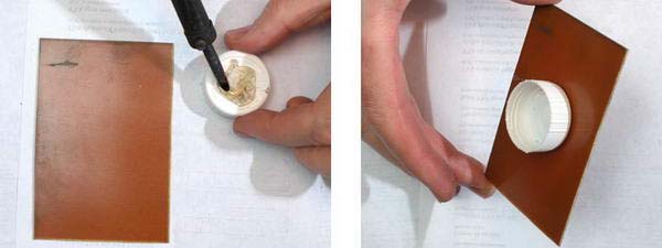
Aligning the top and bottom photomasks on the workpiece surfaces
Each of the photo masks (top and bottom) should have marks along which 2 holes need to be made on the workpiece to align the layers. The farther the marks are from each other, the higher the alignment accuracy. I usually place them diagonally on the templates. Using a drilling machine, using these marks on the workpiece, we drill two holes strictly at 90° (the thinner the holes, the more accurate the alignment; I use a 0.3 mm drill) and align the templates along them, not forgetting that the template must be applied to the photoresist the side on which the print was made. We press the templates to the workpiece with thin glasses. It is preferable to use quartz glass as it transmits ultraviolet radiation better. Plexiglas (plexiglass) gives even better results, but it has the unpleasant property of scratching, which will inevitably affect the quality of the PP. For small PCB sizes, you can use a transparent cover from a CD package. In the absence of such glass, you can use ordinary window glass, increasing the exposure time. It is important that the glass is smooth, ensuring an even fit of the photomasks to the workpiece, otherwise it will be impossible to obtain high-quality edges of the tracks on the finished PCB.

A blank with a photomask under plexiglass. We use a CD box.
Exposure (light exposure)
The time required for exposure depends on the thickness of the photoresist layer and the intensity of the light source. Photoresist varnish POSITIV 20 is sensitive to ultraviolet rays, the maximum sensitivity occurs in the area with a wavelength of 360-410 nm.
It is best to expose under lamps whose radiation range is in the ultraviolet region of the spectrum, but if you do not have such a lamp, you can also use ordinary powerful incandescent lamps, increasing the exposure time. Do not start illumination until the lighting from the source has stabilized; it is necessary for the lamp to warm up for 2-3 minutes. The exposure time depends on the thickness of the coating and is usually 60-120 seconds when the light source is located at a distance of 25-30 cm. The glass plates used can absorb up to 65% of ultraviolet radiation, so in such cases it is necessary to increase the exposure time. The best results are achieved when using transparent plexiglass plates. When using photoresist with a long shelf life, the exposure time may need to be doubled remember: Photoresists are subject to aging!
Examples of using different light sources:


UV lamps
We expose each side in turn, after exposure we let the workpiece stand for 20-30 minutes in a dark place.
Development of the exposed workpiece
We develop it in a solution of NaOH (caustic soda) see the beginning of the article for more details at a solution temperature of 20-25°C. If there is no manifestation within 2 minutes small O exposure time. If it appears well, but useful areas are also washed away you were too clever with the solution (the concentration is too high) or the exposure time with a given radiation source is too long or the photomask is of poor quality the printed black color is not saturated enough to allow ultraviolet light to illuminate the workpiece.
When developing, I always very carefully, effortlessly “roll” a cotton swab on a glass rod over the places where the exposed photoresist should be washed off; this speeds up the process.
Washing the workpiece from alkali and residues of exfoliated exposed photoresist
I do this under the tap with regular tap water.
Re-tanning photoresist
We place the workpiece in the oven, gradually raise the temperature and hold it at a temperature of 60-100°C for 60-120 minutes; the pattern becomes strong and hard.
Checking the development quality
Briefly (for 5-15 seconds) immerse the workpiece in a ferric chloride solution heated to a temperature of 50-60°C. Rinse quickly with running water. In places where there is no photoresist, intensive etching of the copper begins. If photoresist accidentally remains somewhere, carefully remove it mechanically. It is convenient to do this with a regular or ophthalmic scalpel, armed with optics (soldering glasses, magnifying glass A watchmaker, loupe A on a tripod, microscope).
Etching
We poison in a concentrated solution of ferric chloride at a temperature of 50-60°C. It is advisable to ensure continuous circulation of the etching solution. We carefully “massage” poorly bleeding areas with a cotton swab on a glass rod. If ferric chloride is freshly prepared, the etching time usually does not exceed 5-6 minutes. We rinse the workpiece with running water.


Board etched
How to prepare a concentrated solution of ferric chloride? Dissolve FeCl 3 in slightly (up to 40°C) heated water until it stops dissolving. Filter the solution. It should be stored in a cool, dark place in sealed non-metallic packaging in glass bottles, for example.
Removing unnecessary photoresist
We wash off the photoresist from the tracks with acetone or a solvent for nitro paints and nitro enamels.
Drilling holes
It is advisable to select the diameter of the point of the future hole on the photomask such that it will be convenient to drill later. For example, with a required hole diameter of 0.6-0.8 mm, the diameter of the point on the photomask should be about 0.4-0.5 mm in this case the drill will be well centered.
It is advisable to use drills coated with tungsten carbide: drills made of high-speed steels wear out very quickly, although steel can be used for drilling single holes of large diameter (more than 2 mm), since drills coated with tungsten carbide of this diameter are too expensive. When drilling holes with a diameter of less than 1 mm, it is better to use a vertical machine, otherwise your drill bits will break quickly. If you drill with a hand drill, distortions are inevitable, leading to inaccurate joining of holes between layers. The top-down movement on a vertical drilling machine is the most optimal in terms of the load on the tool. Carbide drills are made with a rigid (i.e. the drill fits exactly to the hole diameter) or a thick (sometimes called "turbo") shank that has a standard size (usually 3.5 mm). When drilling with carbide-coated drills, it is important to firmly secure the PCB, since such a drill, when moving upward, can lift the PCB, skew the perpendicularity and tear out a fragment of the board.
Small diameter drills are usually fitted into either a collet chuck (various sizes) or a three-jaw chuck. For precise clamping, clamping in a three-jaw chuck is not the best option, and the small drill size (less than 1 mm) quickly makes grooves in the clamps, losing good clamping. Therefore, for drills with a diameter less than 1 mm, it is better to use a collet chuck. To be on the safe side, purchase an extra set containing spare collets for each size. Some inexpensive drills come with plastic collets; throw them away and buy metal ones.
To obtain acceptable accuracy, it is necessary to properly organize the workplace, that is, firstly, to ensure good lighting of the board when drilling. To do this, you can use a halogen lamp, attaching it to a tripod to be able to choose a position (illuminate the right side). Secondly, raise the work surface about 15 cm above the table top for better visual control over the process. It would be a good idea to remove dust and chips while drilling (you can use a regular vacuum cleaner), but this is not necessary. It should be noted that the dust from fiberglass generated during drilling is very caustic and, if it comes into contact with the skin, causes skin irritation. And finally, when working, it is very convenient to use the foot switch of the drilling machine.
Typical hole sizes:
- vias 0.8 mm or less;
- integrated circuits, resistors, etc. 0.7-0.8 mm;
- large diodes (1N4001) 1.0 mm;
- contact blocks, trimmers up to 1.5 mm.
Try to avoid holes with a diameter of less than 0.7 mm. Always keep at least two spare drills of 0.8 mm or smaller, as they always break just at the moment when you urgently need to order. Drills 1 mm and larger are much more reliable, although it would be nice to have spare ones for them. When you need to make two identical boards, you can drill them simultaneously to save time. In this case, it is necessary to very carefully drill holes in the center of the contact pad near each corner of the PCB, and for large boards, holes located close to the center. Lay the boards on top of each other and, using 0.3mm centering holes in two opposite corners and pins as pegs, secure the boards to each other.
If necessary, you can countersink the holes with larger diameter drills.
Copper tinning on PP
If you need to tin the tracks on the PCB, you can use a soldering iron, soft low-melting solder, alcohol-rosin flux and coaxial cable braid. For large volumes, they tin in baths filled with low-temperature solders with the addition of fluxes.
The most popular and simple melt for tinning is the low-melting alloy “Rose” (tin 25%, lead 25%, bismuth 50%), the melting point of which is 93-96°C. Using tongs, place the board under the level of the liquid melt for 5-10 seconds and, after removing it, check whether the entire copper surface is evenly covered. If necessary, the operation is repeated. Immediately after removing the board from the melt, its remains are removed either using a rubber squeegee or by sharp shaking in a direction perpendicular to the plane of the board, holding it in the clamp. Another way to remove residual Rose alloy is to heat the board in a heating cabinet and shake it. The operation can be repeated to achieve a mono-thickness coating. To prevent oxidation of the hot melt, glycerin is added to the tinning container so that its level covers the melt by 10 mm. After the process is completed, the board is washed from glycerin in running water. Attention! These operations involve working with installations and materials exposed to high temperatures, therefore, to prevent burns, it is necessary to use protective gloves, goggles and aprons.
The operation of tinning with a tin-lead alloy proceeds in a similar way, but the higher temperature of the melt limits the scope of application of this method in handicraft production conditions.
After tinning, do not forget to clean the board from flux and thoroughly degrease it.
If you have a large production, you can use chemical tinning.
Applying a protective mask
The operations with applying a protective mask exactly repeat everything that was written above: we apply photoresist, dry it, tan it, center the mask photomasks, expose it, develop it, wash it and tan it again. Of course, we skip the steps of checking the quality of development, etching, removing photoresist, tinning and drilling. At the very end, tan the mask for 2 hours at a temperature of about 90-100°C - it will become strong and hard, like glass. The formed mask protects the surface of the PP from external influences and protects against theoretically possible short circuits during operation. It also plays an important role in automatic soldering: it prevents the solder from “sitting” on adjacent areas, short-circuiting them.
That's it, the double-sided printed circuit board with mask is ready
I had to make a PP in this way with the width of the tracks and the step between them up to 0.05 mm (!). But this is already jewelry work. And without much effort, you can make PP with a track width and a step between them of 0.15-0.2 mm.
I did not apply a mask to the board shown in the photographs; there was no such need.


Printed circuit board in the process of installing components on it
And here is the device itself for which the PP was made:

This is a cellular telephone bridge that allows you to reduce the cost of mobile communication services by 2-10 times for this it was worth bothering with the PP;). The PCB with soldered components is located in the stand. Previously, there was an ordinary charger for mobile phone batteries.
Additional Information
Metallization of holes
You can even metallize holes at home. To do this, the inner surface of the holes is treated with a 20-30% solution of silver nitrate (lapis). Then the surface is cleaned with a squeegee and the board is dried in the light (you can use a UV lamp). The essence of this operation is that under the influence of light, silver nitrate decomposes, and silver inclusions remain on the board. Next, the chemical precipitation of copper from the solution is carried out: copper sulfate (copper sulfate) 2 g, caustic soda 4 g, ammonia 25 percent 1 ml, glycerin 3.5 ml, formaldehyde 10 percent 8-15 ml, water 100 ml. The shelf life of the prepared solution is very short; it must be prepared immediately before use. After the copper is deposited, the board is washed and dried. The layer turns out to be very thin; its thickness must be increased to 50 microns by galvanic means.
Solution for applying copper plating by electroplating:
For 1 liter of water, 250 g of copper sulfate (copper sulfate) and 50-80 g of concentrated sulfuric acid. The anode is a copper plate suspended parallel to the part being coated. The voltage should be 3-4 V, current density 0.02-0.3 A/cm 2, temperature 18-30°C. The lower the current, the slower the metallization process, but the better the resulting coating.

A fragment of a printed circuit board showing metallization in the hole
Homemade photoresists
Photoresist based on gelatin and potassium bichromate:
First solution: pour 15 g of gelatin into 60 ml of boiled water and leave to swell for 2-3 hours. After the gelatin swells, place the container in a water bath at a temperature of 30-40°C until the gelatin is completely dissolved.
Second solution: dissolve 5 g of potassium dichromate (chrompic, bright orange powder) in 40 ml of boiled water. Dissolve in low, diffused light.
Pour the second into the first solution with vigorous stirring. Using a pipette, add a few drops of ammonia to the resulting mixture until it becomes straw-colored. The emulsion is applied to the prepared board under very low light. The board is dried until it is tack-free at room temperature in complete darkness. After exposure, rinse the board under low ambient light in warm running water until the untanned gelatin is removed. To better evaluate the result, you can paint areas with unremoved gelatin with a solution of potassium permanganate.
Improved homemade photoresist:
First solution: 17 g of wood glue, 3 ml of ammonia aqueous solution, 100 ml of water, leave to swell for a day, then heat in a water bath at 80°C until completely dissolved.
Second solution: 2.5 g potassium dichromate, 2.5 g ammonium dichromate, 3 ml aqueous ammonia solution, 30 ml water, 6 ml alcohol.
When the first solution has cooled to 50°C, pour the second solution into it with vigorous stirring and filter the resulting mixture ( This and subsequent operations must be carried out in a darkened room, sunlight is not allowed!). The emulsion is applied at a temperature of 30-40°C. Continue as in the first recipe.
Photoresist based on ammonium dichromate and polyvinyl alcohol:
Prepare a solution: polyvinyl alcohol 70-120 g/l, ammonium dichromate 8-10 g/l, ethyl alcohol 100-120 g/l. Avoid bright light! Apply in 2 layers: first layer drying 20-30 minutes at 30-45°C second layer drying 60 minutes at 35-45°C. Developer 40% ethyl alcohol solution.
Chemical tinning
First of all, the board must be picked out to remove the formed copper oxide: 2-3 seconds in a 5% solution of hydrochloric acid, followed by rinsing in running water.
It is enough to simply carry out chemical tinning by immersing the board in an aqueous solution containing tin chloride. The release of tin on the surface of a copper coating occurs when immersed in a tin salt solution in which the potential of the copper is more electronegative than the coating material. The change in potential in the desired direction is facilitated by the introduction of a complexing additive, thiocarbamide (thiourea), into the tin salt solution. This type of solution has the following composition (g/l):
Among the listed solutions, solutions 1 and 2 are the most common. Sometimes, the use of Progress detergent in an amount of 1 ml/l is suggested as a surfactant for the 1st solution. Adding 2-3 g/l bismuth nitrate to the 2nd solution leads to the precipitation of an alloy containing up to 1.5% bismuth, which improves the solderability of the coating (prevents aging) and greatly increases the shelf life of the finished PCB before soldering components.
To preserve the surface, aerosol sprays based on fluxing compositions are used. After drying, the varnish applied to the surface of the workpiece forms a strong, smooth film that prevents oxidation. One of the popular substances is “SOLDERLAC” from Cramolin. Subsequent soldering is carried out directly on the treated surface without additional varnish removal. In particularly critical cases of soldering, the varnish can be removed with an alcohol solution.
Artificial tinning solutions deteriorate over time, especially when exposed to air. Therefore, if you have large orders infrequently, then try to prepare a small amount of solution at once, sufficient to tinning the required amount of PP, and store the remaining solution in a closed container (bottles of the type used in photography that do not allow air to pass through are ideal). It is also necessary to protect the solution from contamination, which can greatly degrade the quality of the substance.
In conclusion, I want to say that it is still better to use ready-made photoresists and not bother with metalizing holes at home; you still won’t get great results.
Many thanks to the candidate of chemical sciences Filatov Igor Evgenievich for consultations on issues related to chemistry.
I also want to express my gratitude Igor Chudakov."
Recently, radio electronics as a hobby has been gaining popularity in the world; people are becoming interested in creating electronic devices with their own hands. There are a huge number of circuits on the Internet, from simple to complex, performing various tasks, so everyone can find something they like in the world of radio electronics.
An integral part of any electronic device is a printed circuit board. It is a plate of dielectric material on which copper conductive paths are applied that connect electronic components. Each of those who want to learn how to assemble electrical circuits in a beautiful form must learn how to make these same printed circuit boards.
There are computer programs that allow you to draw a pattern of printed circuit board tracks in a convenient interface, the most popular of which is. The layout of the printed circuit board is carried out in accordance with the circuit diagram of the device; there is nothing complicated about it; you just need to connect the necessary parts with tracks. In addition, many circuit diagrams of electronic devices on the Internet already come with ready-made printed circuit board drawings.
A good printed circuit board is the key to long and happy operation of the device, so you should try to make it as carefully and efficiently as possible. The most common method of making printed ones at home is the so-called “”, or “laser-ironing technology”. It has gained wide popularity because it does not take much time, does not require scarce ingredients, and is not so difficult to learn. Briefly, LUT can be described as follows: let's say there is a pattern of tracks drawn on a computer. Next, this drawing needs to be printed on special thermal transfer paper, transferred to textolite, then the excess copper must be etched from the board, holes drilled in the right places and the tracks tinned. Let's look at the whole process step by step:
Printing a board design
1) Printing a design on thermal transfer paper. You can buy such paper, for example, on Aliexpress, where it costs mere pennies - 10 rubles per A4 sheet. Instead, you can use any other glossy paper, for example, from magazines. However, the quality of toner transfer from such paper may be much worse. Some people use glossy photo paper "Lomond", a good option, if not for the price - such photo paper is much more expensive. I recommend trying to print the drawing on different papers, and then compare which one produces the best result.
Another important point when printing a picture is the printer settings. It is imperative to disable toner saving, but the density should be set to maximum, because the thicker the toner layer, the better for our purposes.

You also need to take into account the fact that the design will be transferred to the textolite in a mirror image, so you need to foresee in advance whether or not you need to mirror the design before printing. This is especially critical on boards with microcircuits, because it will not be possible to install them on the other side.

Preparing PCB for transferring a drawing onto it
2) The second stage is preparing the textolite for transferring the drawing onto it. Most often, textolite is sold in pieces measuring 70x100 or 100x150 mm. You need to cut a piece that fits the dimensions of the board, with a margin of 3-5 mm at the edges. It is most convenient to saw PCB with a hacksaw or a jigsaw; in extreme cases, it can be cut off with metal scissors. Then, this piece of PCB should be wiped with fine sandpaper or a hard eraser. Small, small scratches will form on the surface of the copper foil; this is normal. Even if the PCB initially looks perfectly smooth, this step is necessary, otherwise it will be difficult to tin it later. After sanding, the surface must be wiped with alcohol or solvent to wash off dust and greasy hand marks. After this, you cannot touch the copper surface.


Transferring the drawing to the prepared textolite
3) The third stage is the most critical. It is necessary to transfer the drawing printed on thermal transfer paper to the prepared textolite. To do this, cut the paper as shown in the photo, leaving some margin around the edges. On a flat wooden board we place the paper with the pattern facing up, then we apply textolite on top, copper to the paper. We bend the edges of the paper as if it were hugging a piece of PCB. After this, carefully turn the sandwich over so that the paper is on top. We check that the drawing has not shifted anywhere relative to the PCB and place a clean piece of ordinary office white paper on top so that it covers the entire sandwich.


Now all that remains is to heat the whole thing thoroughly, and all the toner from the paper will end up on the PCB. You need to apply a heated iron on top and heat the sandwich for 30-90 seconds. The heating time is selected experimentally and largely depends on the temperature of the iron. If the toner transfers poorly and remains on the paper, you need to keep it longer, but if, on the contrary, the tracks transfer, but are smeared, this is a clear sign of overheating. There is no need to put pressure on the iron; its own weight is enough. After warming up, you need to remove the iron and iron the still hot workpiece with a cotton swab, in case in some places the toner did not transfer well when ironing. After this, all that remains is to wait until the future board cools down and remove the thermal transfer paper. It may not work out the first time, it doesn’t matter, because experience comes with time.
PCB etching
4) The next stage is etching. Any area of copper foil that is not covered by toner should be removed, leaving the copper underneath the toner untouched. First you need to prepare a solution for etching copper; the simplest, most accessible and cheapest option is a solution of citric acid, salt and hydrogen peroxide. In a plastic or glass container you need to mix one or two tablespoons of citric acid and a teaspoon of table salt per glass of water. Proportions do not play a big role, you can pour it by eye. Mix thoroughly and the solution is ready. You need to put the board in it, tracks down, to speed up the process. You can also slightly warm the solution, this will further increase the speed of the process. After about half an hour, all the excess copper will be etched away and only the tracks will remain.


Wash toner off tracks
5) The hardest part is over. At the fifth stage, when the board is already etched, you need to wash off the toner from the tracks with a solvent. The most affordable option is women's nail polish remover; it costs a penny and almost every woman has it. You can also use common solvents, such as acetone. I use petroleum solvent; although it stinks a lot, it doesn’t leave any black marks on the board. As a last resort, you can remove the toner by thoroughly rubbing the board with sandpaper.

Drilling holes on the board
6) Drilling holes. You will need a small drill with a diameter of 0.8 - 1 mm. Conventional high-speed steel drills quickly become dull on PCB, so it is best to use tungsten carbide drills, although they are more fragile. I drill boards using a motor from an old hair dryer with a small collet chuck; the holes are smooth and without burrs. Unfortunately, the last carbide drill bit broke at the most inopportune moment, so only half of the holes are drilled in the photos. The rest can be drilled later.


Tin the tracks
7) All that remains is to tin the copper tracks, i.e. cover with a layer of solder. Then they will not oxidize over time, and the board itself will become beautiful and shiny. First you need to apply flux to the tracks, and then quickly move a soldering iron with a drop of solder over them. You should not apply an excessively thick layer of solder, otherwise the holes may close and the board will look sloppy.

At this point, the manufacturing process of the printed circuit board is completed, and now you can solder parts into it. Material provided for the Radioschemes website by Mikhail Gretsky, [email protected]
Discuss the article MANUFACTURING PRINTED BOARDS WITH LUT
In this post, I will analyze popular methods for creating printed circuit boards yourself at home: LUT, photoresist, hand drawing. And also what programs are best to draw PP.
Once upon a time, electronic devices were mounted using surface mounting. Nowadays, only tube audio amplifiers are assembled this way. Printed editing is in widespread use, which has long turned into a real industry with its own tricks, features and technologies. And there are a lot of tricks there. Especially when creating PCBs for high-frequency devices. (I think I’ll do a review of the literature and features of designing the location of PP conductors someday)
The general principle of creating printed circuit boards (PCBs) is to apply tracks on a surface made of non-conducting material that conduct this current. The tracks connect the radio components according to the required circuit. The result is an electronic device that can be shaken, carried, and sometimes even wet without fear of damaging it.
In general terms, the technology for creating a printed circuit board at home consists of several steps:
- Select a suitable foil fiberglass laminate. Why textolite? It's easier to get. Yes, and it turns out cheaper. Often this is enough for an amateur device.
- Apply a printed circuit board design to the PCB
- Bleed off excess foil. Those. remove excess foil from areas of the board that do not have a conductor pattern.
- Drill holes for component leads. If you need to drill holes for components with leads. This is obviously not required for chip components.
- Tin the current-carrying paths
- Apply solder mask. Optional if you want to make your board look closer to the factory ones.
Another option is to simply order the board from the factory. Nowadays, many companies provide printed circuit board production services. You will receive an excellent factory printed circuit board. They will differ from amateur ones not only in the presence of a solder mask, but also in many other parameters. For example, if you have a double-sided PCB, then the board will not have metallization of the holes. You can choose the solder mask color, etc. There are a lot of advantages, just have time to slobber on the money!
Step 0
Before making a PCB, it must be drawn somewhere. You can draw it the old fashioned way on graph paper and then transfer the drawing to the workpiece. Or you can use one of the many programs for creating printed circuit boards. These programs are called the general word CAD (CAD). Some of the options available to a radio amateur include DeepTrace (free version), Sprint Layout, Eagle (you can, of course, also find specialized ones like Altium Designer)
Using these programs, you can not only draw a PCB, but also prepare it for production in a factory. What if you want to order a dozen scarves? And if you don’t want to, then it’s convenient to print such a PP and make it yourself using LUT or photoresist. But more on that below.
Step 1
So, the workpiece for PP can be divided into two parts: a non-conductive base and a conductive coating.

There are different blanks for PP, but most often they differ in the material of the non-conductive layer. You can find such a substrate made of getinax, fiberglass, a flexible base made of polymers, compositions of cellulose paper and fiberglass with epoxy resin, and even a metal base. All these materials differ in their physical and mechanical properties. And in production, the material for PP is selected based on economic considerations and technical conditions.

For home PP, I recommend foil fiberglass. Easy to get and reasonably priced. Getinaks are probably cheaper, but personally I can’t stand them. If you've disassembled at least one mass-produced Chinese device, you've probably seen what the PCBs are made of? They are brittle and stink when soldered. Let the Chinese smell it.

Depending on the device being assembled and its operating conditions, you can choose the appropriate PCB: single-sided, double-sided, with different foil thicknesses (18 microns, 35 microns, etc., etc.
Step 2
To apply a PP pattern to a foil base, radio amateurs have developed many methods. Among them are the two most popular at the present time: LUT and photoresist. LUT is an abbreviation for laser ironing technology. As the name suggests, you will need a laser printer, an iron and glossy photo paper.
LUT
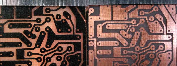
A mirrored image is printed onto photographic paper. Then it is applied to foil PCB. And it warms up well with an iron. When exposed to heat, toner from glossy photo paper sticks to the copper foil. After warming up, the board is soaked in water and the paper is carefully removed.

The photo above shows the board after etching. The black color of the current paths is due to the fact that they are still covered with hardened toner from the printer.
Photoresist
This is a more complex technology. But with its help you can get a better result: without mordants, thinner tracks, etc. The process is similar to LUT, but the PP design is printed on transparent film. This creates a template that can be used over and over again. Then a “photoresist” is applied to the PCB—an ultraviolet-sensitive film or liquid (photoresist can be different).
Then a photomask with a PP pattern is firmly fixed on top of the photoresist and then this sandwich is irradiated with an ultraviolet lamp for a clearly measured time. It must be said that the PP pattern on the photomask is printed inverted: the paths are transparent and the voids are dark. This is done so that when the photoresist is exposed to light, the areas of the photoresist not covered by the template react to ultraviolet radiation and become insoluble.
After exposure (or exposure, as the experts call it), the board “develops” - the exposed areas become dark, the unexposed areas become light, since the photoresist there has simply dissolved in the developer (ordinary soda ash). Then the board is etched in a solution, and then the photoresist is removed, for example, with acetone.
Types of photoresist
There are several types of photoresist in nature: liquid, self-adhesive film, positive, negative. What is the difference and how to choose the right one? In my opinion, there is not much difference in amateur use. Once you get the hang of it, you’ll use that type. I would highlight only two main criteria: price and how convenient it is for me personally to use this or that photoresist.
Step 3
Etching of a PP blank with a printed pattern. There are many ways to dissolve the unprotected part of the PP foil: etching in ammonium persulfate, ferric chloride, . I like the last method: fast, clean, cheap.
We place the workpiece in the etching solution, wait 10 minutes, remove it, wash it, clean the tracks on the board and move on to the next stage.
Step 4
The board can be tinned with either Rose or Wood alloy, or simply cover the tracks with flux and go over them with a soldering iron and solder. Rose and Wood alloys are multicomponent low-melting alloys. And Wood's alloy also contains cadmium. So, at home, such work should be carried out under a hood with a filter. It is ideal to have a simple smoke extractor. You want to live happily ever after? :=)
Step 6
I will skip the fifth step, everything is clear there. But applying a solder mask is quite an interesting and not the easiest stage. So let's study it in more detail.
A solder mask is used in the process of creating a PCB in order to protect the board tracks from oxidation, moisture, fluxes when installing components, and also to facilitate the installation itself. Especially when SMD components are used.
Usually, to protect PP tracks without a mask from chemicals. and to avoid exposure, seasoned radio amateurs cover such tracks with a layer of solder. After tinning, such a board often does not look very nice. But what’s worse is that during the tinning process you can overheat the tracks or hang “snot” between them. In the first case, the conductor will fall off, and in the second, such unexpected “snot” will have to be removed in order to eliminate the short circuit. Another disadvantage is the increase in capacitance between such conductors.
First of all: solder mask is quite toxic. All work should be carried out in a well-ventilated area (preferably under a hood), and avoid getting the mask on the skin, mucous membranes and eyes.
I can’t say that the process of applying the mask is quite complicated, but it still requires a large number of steps. After thinking about it, I decided that I would give a link to a more or less detailed description of applying a solder mask, since there is no way to demonstrate the process on my own right now.
Get creative, guys, it's interesting =) Creating PP in our time is akin to not just a craft, but an entire art!
Homemade printed circuit board
How to make a printed circuit board at home using laser-iron technology. This refers to the thermal transfer of toner from paper to the metallization surface of the future printed circuit board.
I tried many times to make a printed circuit board using laser-iron technology, but I never managed to get a reliable, easily repeatable result. In addition, when making a board, I need etched holes in the pads no larger than 0.5 mm in size. Subsequently, I use them when drilling, in order to center a drill with a diameter of 0.75 mm.
Defects manifest themselves in the form of a shift or change in the width of the tracks, as well as in the unequal thickness of the toner remaining on the copper foil after removing the paper. In addition, when removing the paper before etching, it is problematic to clean every hole in the toner of cellulose residue. As a result, when etching a printed circuit board, additional difficulties arise, which were avoided only by doing the opposite. http://oldoctober.com/ru/
I assume that the reason causing the marriage is the following.
Paper, when heated to a high temperature, begins to warp. While the temperature of foil fiberglass is always slightly lower. The toner partially adheres to the foil, but remains melted on the paper side. When warped, the paper moves and changes the original shape of the conductors.
At the very beginning, I want to warn you that the technology is not without certain disadvantages.
The first is the lack of special paper for thermal transfer, instead of which I suggest choosing suitable paper for self-adhesive labels. Unfortunately, not all paper is suitable. You need to choose one whose labels are denser and the backing has a good, smooth surface.
The second disadvantage is that the size of the printed circuit board is limited by the size of the soleplate of the iron. In addition, not every iron can heat foil fiberglass laminate evenly enough, so it is better to choose the most massive one.
However, despite all these shortcomings, the technology described below allowed me to obtain a stable, easily repeatable result in small-scale production.
The essence of the change in the traditional process is that it is proposed to heat not the paper with toner, but the foil fiberglass itself.
The main advantage is that with this method it is easy to control the temperature in the toner melting zone. In addition, the rubber roller allows you to evenly distribute the pressure and prevent crushing of the toner. (I write everywhere about foil fiberglass, since I have not tested other materials).
The technology is equally well suited for foil fiberglass laminate of different thicknesses, but it is better to use material no thicker than one millimeter, as it is easy to cut with scissors.
So, we take a piece of the most shabby foil fiberglass laminate and process it with sandpaper. You should not use very large sandpaper, as it can damage future tracks. However, you don’t have to sand it if you have a piece of new fiberglass. The copper surface must be thoroughly cleaned and degreased in any case.

Making a stencil for thermal transfer. To do this, we cut off the required piece from a sheet of paper for labels and separate the labels themselves from the backing. You should leave a piece of label at the beginning of the sheet to prevent the backing from getting stuck in the printer mechanism.
Do not touch with your hands the areas on the substrate where toner will subsequently be applied.

If the thickness of the foil fiberglass laminate is one millimeter or less, then the distance between the edges of the individual boards can be chosen to be 0.2 mm; if it is larger and you are going to cut the workpiece with a hacksaw, then 1.5-2.0 mm, depending on the thickness of the blade and processing tolerance.

I use the toner layer that is installed by default in the printer driver, but “B & W Halftones:” (B/W Halftone) should be selected “Solid”. In other words, you need to prevent the appearance of a raster. You may not see it on the stencil, but it may affect the thickness of the toner.

We fix the stencil on a piece of foil fiberglass with paper clips. We attach another paper clip to the free edge of the stencil so that it does not come into contact with the iron.
The melting point of different brands of toner is approximately 160-180C. Therefore, the temperature of the iron should be slightly higher by 10-20C. If your iron does not heat up to a temperature of 180C, then you will have to adjust it.

Before heating, the soleplate of the iron should be thoroughly cleaned of grease and other contaminants!
We heat the iron to a temperature of 180-190 degrees and press it tightly against the foil fiberglass as shown in the figure. If you position the iron differently, the board may heat up too unevenly, since usually the iron heats up 20-30C more in the wide part. Wait two minutes.

After this, remove the iron and in one motion, forcefully roll the stencil onto the foil fiberglass using a rubber roller for rolling photographs.
If during rolling the toner is crushed, that is, the tracks move to the side or change their shape, then you should reduce the amount of toner in the printer driver.
It is necessary that the center of the roller always moves along the center of the board. The roller handle must be held in such a way as to prevent the appearance of a force vector directed “around” the handle.

We roll the stencil tightly a few more times and press the resulting “sandwich” with something heavy, after laying down a newspaper folded several times in order to evenly distribute the weight.
The stencil should be rolled in the same direction each time. The roller begins to move from the place where the stencil is attached.

After about ten minutes you can remove the press and remove the stencil. This is what happened.


Now you need to glue something to the back side of the board in any way so that you can later hold this board during etching. (I use hot glue.)
We etch the board in a ferric chloride solution.
How to prepare the solution?
If a jar of ferric chloride is unsealed, then most likely there is already a super-concentrated solution there. It can be poured into a pickling bowl and a little water added.
If ferric chloride has not yet been covered with water, you can do it yourself. You can probably get the crystals themselves out of the jar, but don’t use heirloom silver for this.
Keep in mind that the etching process will not work in a highly concentrated solution, so once you have such a solution, you need to add a little water.
It is best to use a vinyl plastic photo bath as a dish, but you can use any other one.
The picture shows that the board floats on the surface of the solution due to its surface tension. This method is good because the etching products do not linger on the surface of the board, but immediately sink to the bottom of the bath.

At the very beginning of etching, you need to make sure that there are no air bubbles left under the board. During the etching process, it is advisable to check that the etching proceeds evenly over the entire surface of the board.
If there is any heterogeneity, then you need to activate the process with an old toothbrush or something similar. But this must be done carefully so as not to destroy the toner layer.
Particular attention should be paid to the holes in the contact pads. The areas where the etching process did not start immediately are lighter. In principle, it is enough to darken the entire surface and all holes at the very beginning of the process, and then success is a foregone conclusion.

If the main part of the board was etched in 15 minutes, then you should not increase the total etching time more than twice, that is, more than 30 minutes. Further etching will not only reduce the width of the conductors, but may also partially destroy the toner.
Typically, all 0.5mm holes in the contact pads are etched in twice the time.
The motor turns a small eccentric, which creates vibrations in the solution (not necessary if you periodically lift and move the board).
Wash off the toner with a swab soaked in acetone.
This is what happened. On the left, the board is still covered with toner. The width of the tracks is 0.4mm.

Now you can remove the burrs formed on the copper during drilling. To do this, we first roll them up using a ball bearing secured in some convenient mandrel. In this case, it is better to place the board on a hard, flat surface. Then, using fine sandpaper, remove oxide from the surface of the copper, if it has formed.

We tin the workpiece, for which we first coat it with a layer of flux.


I went to the office supply store and took a photo of the packaging with Self-adhesive labels. This paper is not suitable for thermal transfer. Although, if there is no other one, then you can use this one after some modification.

The paper that turned out to be the most convenient for thermal transfer was produced by the Finnish company Campas. And since there are no identifying marks on the small packaging, it is unlikely to be identified without testing.
Very often, in the process of technical creativity, it is necessary to make printed circuit boards for mounting electronic circuits. And now I will tell you about one of the most, in my opinion, advanced methods of making printed circuit boards using a laser printer and an iron. We live in the 21st century, so we will make our work easier by using a computer.
Step 1: PCB Design
We will design the printed circuit board using a specialized program. For example, in the program sprint Layout 4.

Step 2: Print the board design
After that, we need to print the board design. To do this we will do the following:
- In the printer settings, we will disable all toner saving options, and if there is a corresponding regulator, we will set the saturation to maximum.
- Let's take an A4 sheet from some unnecessary magazine. The paper should be coated and preferably have a minimum of drawing on it.
- Let's print the PCB design on coated paper in a mirror image. Better in several copies at once.

Step 3. Stripping the board
Let's put the printed sheet aside for now and start preparing the board. Foil getinaks and foil PCB can serve as the starting material for the board. During long-term storage, copper foil becomes covered with a film of oxides, which can interfere with etching. So let's start preparing the board. Use fine sandpaper to remove the oxide film from the board. Don't try too hard, the foil is thin. Ideally, the board should shine after cleaning.

Step 4. Degreasing the board
After cleaning, rinse the board with running water. After this, you need to degrease the board so that the toner sticks better. You can degrease it with any household detergent, or by washing it with an organic solvent (for example, gasoline or acetone).

Step 5. Transferring the drawing to the board
After this, using an iron, we transfer the drawing from the sheet to the board. Let's put the printed pattern on the board and start ironing it with a hot iron, uniformly heating the entire board. The toner will begin to melt and stick to the board. The heating time and force are selected experimentally. It is necessary that the toner does not spread, but it is also necessary that it is completely welded.

Step 6: Clear the paper from the board
After the board with the paper stuck to it has cooled down, we wet it and roll it with our fingers under a stream of water. Wet paper will pellet, but stuck toner will remain in place. The toner is quite strong and is difficult to scrape off with your fingernail.

Step 7. Etch the board
Etching printed circuit boards is best done in ferric chloride (III) Fe Cl 3. This reagent is sold in any radio parts store and is inexpensive. We immerse the board in the solution and wait. The etching process depends on the freshness of the solution, its concentration, etc. May take from 10 minutes to an hour or more. The process can be speeded up by shaking the bath with the solution.

The end of the process is determined visually - when all unprotected copper is removed.

The toner is washed off with acetone.

Step 8: Drilling Holes
Drilling is usually carried out with a small motor with a collet chuck (all this is available in the radio parts store). The diameter of the drill for ordinary elements is 0.8 mm. If necessary, holes are drilled with a large diameter drill.